
Applications
Semiconductor
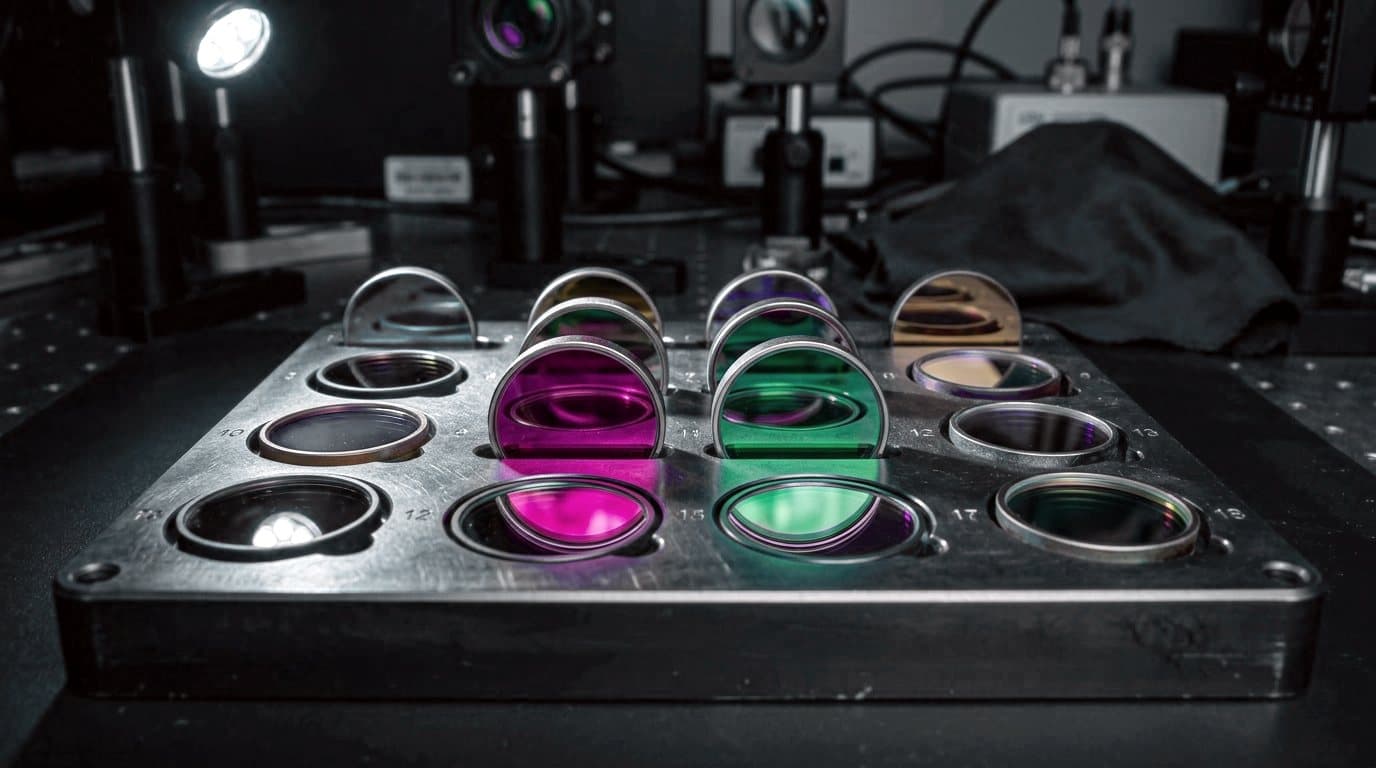
Precision optical windows, carrier plates and specification-driven surface treatments for semiconductor production equipment, each batch delivered with a measurement report.
We supply precision optical components and surface treatment for semiconductor production equipment. Coating thickness is verified by X-RAY and eddy-current methods; every part ships with its measurement record.
What we supply to this sector
- Windows and coatings for equipment optics
- High-purity gold, silver and copper plating
- Thickness verification: ASTM-B499 (X-RAY), ASTM-E376 (eddy-current)
Related capabilities
Frequently asked questions
What do you supply to semiconductor equipment makers?
Reference flats, windows and coated optical components, plus surface treatment (anodizing, electroless nickel, passivation) on equipment parts.
How are cleanliness and particle requirements met?
Optical parts are packed in a clean environment; surface quality is reported in ISO 10110 scratch-dig notation.
Have a drawing for this process?
Send your technical drawing or 3D CAD model through our secure channel. Our engineering team replies with a quotation against the specification.